
There is a very important circuit in the design of the display driver board-the backlight driver circuit, which is also a basic circuit that troubles many engineers. This article will tell you in detail from the backlight unit composition to the backlight circuit design by analyze this circuit step by step. First look at the picture below.

The above picture is the backlight driver circuit diagram of a display screen (AUO M190ETN01.0 ,19") I designed before. This article is going to take this as an example to explain how to design an LED backlight driver circuit and the related principles behind it.
Analysis of backlight unit composition
1. Basic principle analysis
Large-size display screens are currently mainly LCDs. The LCD itself does not emit light. If you want to display pictures, you must use white light backlights. Common white light backlights generally consist of several white LED lights. The number is determined by the size of the screen, generally from 1 to 10 strings (series type, this article does not introduce parallel type), each string ranges from 2 to 20.
2. LED parameters
The main parameters of LED are Vf and If.
Take the commonly used LED for LCD backlighting of ordinary mobile phones as an example. When it emits light normally, its If is 20mA and Vf is generally 3.0~3.4V.
3. Basic design requirements of LED drive circuit
(1) Meet the brightness requirements of the backlight;
(2) The brightness of the entire display is uniform (it is not allowed to have one part brighter and the other part darker);
(3) Brightness can be easily adjusted;
(4) The drive circuit occupies a small PCB space;
(5) High work efficiency;
(6) Low comprehensive cost;
(7) Small interference to other modules of the system.
4. Backlight driving principle
The series drive circuit, as the name implies, in the circuit, the LED lights are connected in series, so the current through each lamp is the same, so as to ensure that the brightness of each lamp is the same, and conclusions can be drawn from it , Uniform brightness is the biggest advantage of tandem type.
Since the lamps are connected in series, and the Vf voltage of each lamp is 3.0~3.4V, taking Vf of 3.0V as an example, if 10 lamps are connected in series, it means that 10*3.0=30V is required. Therefore, the driving circuit of this method needs using DC/DC Boost circuit to boost the voltage to the required voltage.
The figure below is a description in the M190ETN01.0 datasheet.
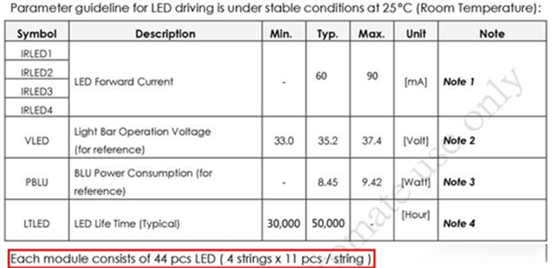
M190ETN01.0 datasheet
The schematic diagram is as follows.
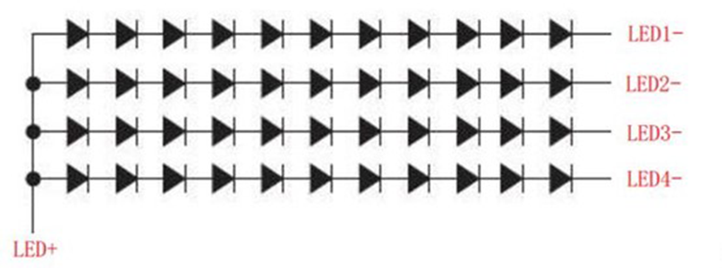
The schematic diagram
There are 4 LED strings in the picture, the positive pole of each string is connected to the high voltage, and the negative pole is led out separately.
Circuit principle analysis
As can be seen from the above figure, the Vmax of the M190ETN01.0 display is 37.4V, and a total of 4 power supplies are required, and the single Imax is 90mA. Therefore, when choosing a boost chip, you can consider two chips with an Imax of 180mA or Consider 4 chips with Imax of 90mA.
Considering some worst cases, we generally need to derate when we choose Boost chips, that is, Vmax and Imax need to be increased by about 50% (need to adjust the derating percentage according to the application environment, because my circuit is used on high-speed rail, derating The amount is slightly larger).
In addition, we have to consider the balance value between each channel. If the value is larger, the brightness uniformity between each channel is worse. Another point is that I personally think that the brightness consistency of the 2-channel 180mA and the 4-channel 90mA will be slightly worse. Comprehensive practical application, we use a one-drive-one approach. The Boost chip selected in this design is MP3394. So far, I don’t know if you have anything you didn’t understand? If not, we continue to analyze.
1. MP3394 function analysis
First paste the function description in the MP3394 datasheet.
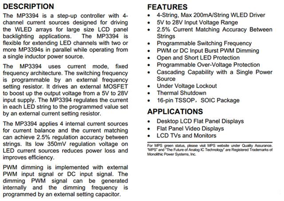
the MP3394 datasheet
The general meaning of the description is: MP3394 is a commonly used LED driver chip, which has 4 output pins and can drive 4 channels at the same time (note that there are 4 channels here, not four strings. It is also mentioned above that according to the current difference, each channel can be simultaneously Drive multiple strings) LED group, the maximum drive current of each channel is 200mA. In order to automatically stabilize the current of the LED lamp to a constant level, a booster is designed to supply power to the LED light bar. The frequency of the booster is fixed, and the frequency can be set by an external resistor. In addition, an external power MOS tube is required to complete the boost conversion.
The drive current of each LED can also be set by an external resistor. There are 4 current sources in the chip to balance the 4 LED currents equally, and the unbalance between each channel is less than 2.5%. This chip can also be dimmed in two different ways: PWM pulse width and DC (current mode).
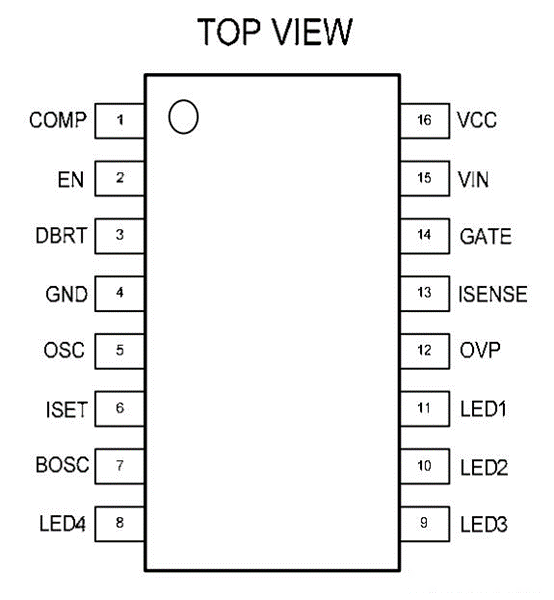
2. Pin function analysis
Since the LED driver chip is a dedicated DCDC chip, the chip pin names of various manufacturers may be inconsistent, but the basic functions are similar. The main pins of MP3394 are analyzed one by one below.
3. In-depth analysis of working principle
The following figure is the internal block diagram of MP3394, just for simple analysis.
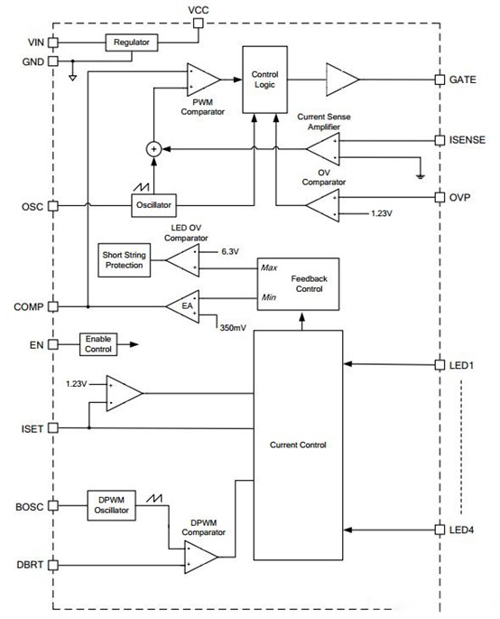
the internal block diagram of MP3394
In the above figure, the backlight power supply is added to the VIN pin of the chip. After the internal voltage is stabilized, the VCC pin gets a regulated 5V voltage, which is used by the internal circuit of the chip. After the chip starts to work, under the action of the internal clock, a high level is output from the GATE pin and added to the G pole of the boost switch tube, and the boost switch tube is turned on.
The rest of the working principle is basically the same as the conventional DCDC, and the rest of the design can be completed by comparing the datasheet, and no detailed analysis of how each device is selected. The following is a detailed analysis of how the brightness is adjusted.
4. Backlight LED brightness adjustment method
Currently, there are two commonly used backlight LED brightness adjustment methods, one is PWM (voltage mode), and the other is DC (current mode).
Compared with voltage mode, the current mode has a faster load response, but the working principle is more complicated. This article will not do research and analysis yet focusing on the analysis of PWM adjustment.
PWM is pulse width modulation. This dimming method uses the duty cycle of the PWM signal to adjust the brightness of the backlight. The frequency and duty cycle of the signal can be set by software. The maximum current Imax is generally set by hardware, and then the actual current flowing through the LED is adjusted by setting the PWM duty cycle; when the duty cycle is 100%, the actual current flowing through the LED is Imax; when the duty cycle is At 50%, the actual current flowing through the LED is 50% of Imax.
Understand from another aspect, the LED backlight drive circuit is actually a steady current circuit, because it can stabilize the current of the LED string at the rated current of the LED lamp. And the magnitude of the current does not change with the brightness of the backlight, that is, when the brightness of the backlight is adjusted, the current of the LED string is stable and always remains at Imax, only by adjusting the time and duty of the LED string to turn on and off To adjust the brightness of the backlight, the current value measured by the ammeter is actually the average current.
For other functions like open circuit, overvoltage, and short circuit protection, you can refer to the explanation in the datasheet. Generally, there is no need to pay too much attention to them in conventional designs.
The last point is that a power inductor and a Schottky diode are needed in the series backlight circuit. Like conventional DCDC, loop problems need to be dealt with during design, otherwise EMI problems will easily occur.
Conclusion
Due to the high failure rate of the LED light bar itself, it often causes the backlight driver board to malfunction. If the backlight driver board itself has any flaws, it will cause serious consequences. Generally, these faults do not appear obviously in the early stage of product work, but often appear in the middle and late stages.
Therefore, it is absolutely necessary for us to understand the principle of this circuit in the design. Different types of displays should be treated differently. Do not blindly apply reference designs. As can be seen in the above analysis, a difference in resistance value will cause abnormal backlight or overload work.


 ipv6 network supported
 online service
 0086-591-8806 9579 88067049
 izzy@lexinda.com
 sarahlpr
 86-15336506363
 English
 Deutsch
 日本語
日本語